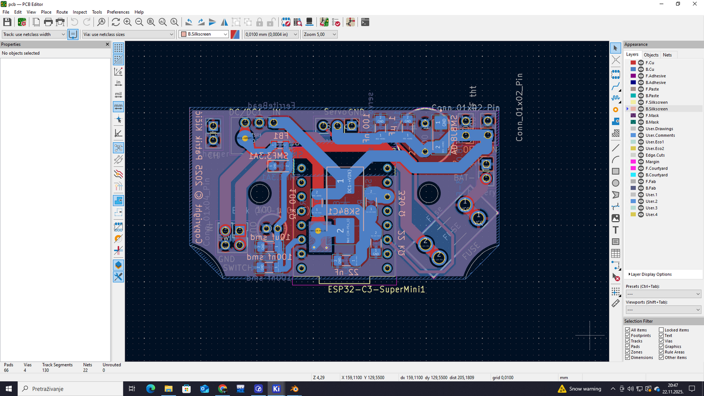
I design simple and clean PCB layouts and schematics in KiCad, perfect for sensor modules, drivers, and small control circuits. Whether you need a basic schematic, a routed PCB, or full production-ready Gerber files, I can help turn your idea into a functional board.
I focus on clear component placement, clean routing, and easy-to-understand schematics ideal for prototypes, DIY electronics, and small embedded systems.
What I offer:
KiCad schematic design
1-layer or 2-layer PCB layout
Clean routing and organized components
Gerber files for fabrication
BOM (Bill of Materials)
PDF schematic (on request)
Simple ESP32 or sensor integration
If you need a small, reliable PCB designed quickly and clearly, I can help.